
您所在的当前位置:首页 > 注意事项
1. Verify that the greatest continuous unpierced area of conductor does not exceed the maximum area diameter specified in Table I of the descriptive pages in this
检测最大的连续未穿孔的导体面积没有超过此步骤中描述页面的表格 I中规定的最大直径面积
COMPONENT - PRINTED WIRING BOARDS (ZPMV2, ZPMV3)
Procedure.This may be accomplished by determining the largest circle which can be inscribed on the unpierced conductor portion of the printed wiring board (see Figure 1.)
步骤:这个可以通过限定最大圆可以内切于未穿孔的印制电路板导体区域来完成(如图:Figure 1)
Figure 1
MAXIMUM UNPIERCED AREA
DIAMETER MEASUREMENT
最大未穿孔面积直径测量
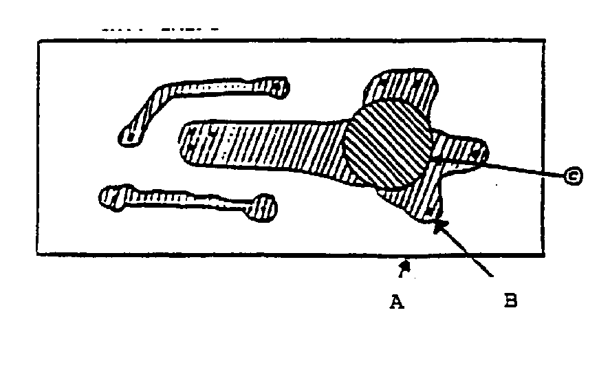
A - Production printed wiring board.
生产印制线路板
B - Largest unpierced conductor section.
最大未穿孔导体区域
C - Largest circle that can be inscribed on B.
能内切于B的最大圆(25.4mm)
如果大于25.4mm可以在铜面中间削一个小圆,来解决此相关规定
板内设计最细线宽0.11MM 离板边最近最细线宽0.17MM
MIDBOARD CONDUCTOR - A conductor spaced more than 1/64 in. (0.4 mm) from the edge of a printed wiring board.
板中导体-导体离印制线路板边缘大于1/64英寸(0.4mm)
如图
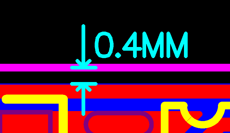
因机床正负0.2MM公差设计时建议大于0.6MM才能保证每PCSW符合UL规定。
检测最大的连续未穿孔的导体面积没有超过此步骤中描述页面的表格 I中规定的最大直径面积
COMPONENT - PRINTED WIRING BOARDS (ZPMV2, ZPMV3)
Procedure.This may be accomplished by determining the largest circle which can be inscribed on the unpierced conductor portion of the printed wiring board (see Figure 1.)
步骤:这个可以通过限定最大圆可以内切于未穿孔的印制电路板导体区域来完成(如图:Figure 1)
Figure 1
MAXIMUM UNPIERCED AREA
DIAMETER MEASUREMENT
最大未穿孔面积直径测量
A - Production printed wiring board.
生产印制线路板
B - Largest unpierced conductor section.
最大未穿孔导体区域
C - Largest circle that can be inscribed on B.
能内切于B的最大圆(25.4mm)
如果大于25.4mm可以在铜面中间削一个小圆,来解决此相关规定
板内设计最细线宽0.11MM 离板边最近最细线宽0.17MM
MIDBOARD CONDUCTOR - A conductor spaced more than 1/64 in. (0.4 mm) from the edge of a printed wiring board.
板中导体-导体离印制线路板边缘大于1/64英寸(0.4mm)
如图
因机床正负0.2MM公差设计时建议大于0.6MM才能保证每PCSW符合UL规定。